
服務(wù)熱線

如何降低電氣成套設(shè)備的電磁干擾
發(fā)布時(shí)間:2025-05-20 來(lái)源:http://www.key126.com/ 瀏覽量:

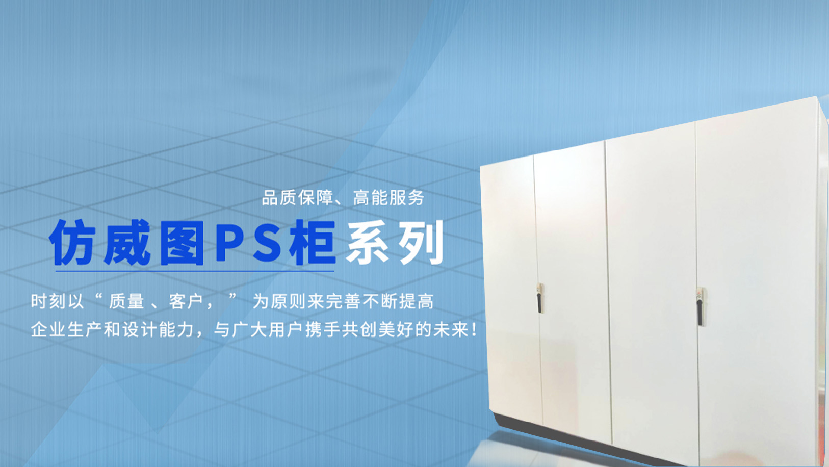
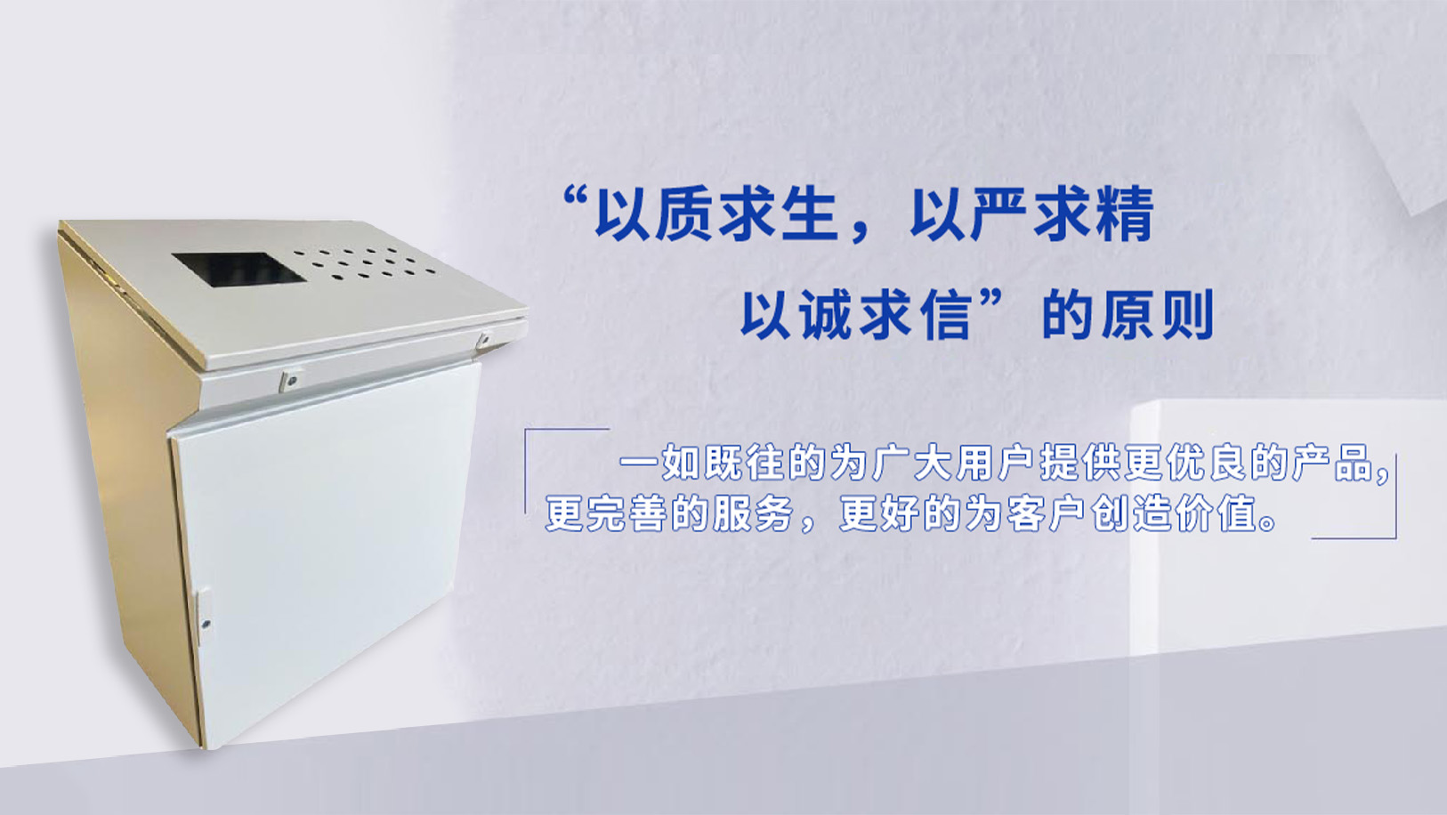
熱門(mén)產(chǎn)品 / HOT PRODUCT
新聞 / NEWS RECOMMENDATIONS
 公司地址:濟(jì)南市槐蔭區(qū)經(jīng)十西路3788號(hào)
 備案號(hào):魯ICP備09028695號(hào)-3
魯公網(wǎng)安備37010402441282號(hào)
備案號(hào):魯ICP備09028695號(hào)-3
魯公網(wǎng)安備37010402441282號(hào)
關(guān)")


南機(jī)箱機(jī)柜")

柜")


 TEL:0531-69922480 18866409905
 EMAIL:
") 首頁(yè)
首頁(yè)品") 產(chǎn)品
產(chǎn)品 電話
電話 置頂
置頂